
Recently added item(s)
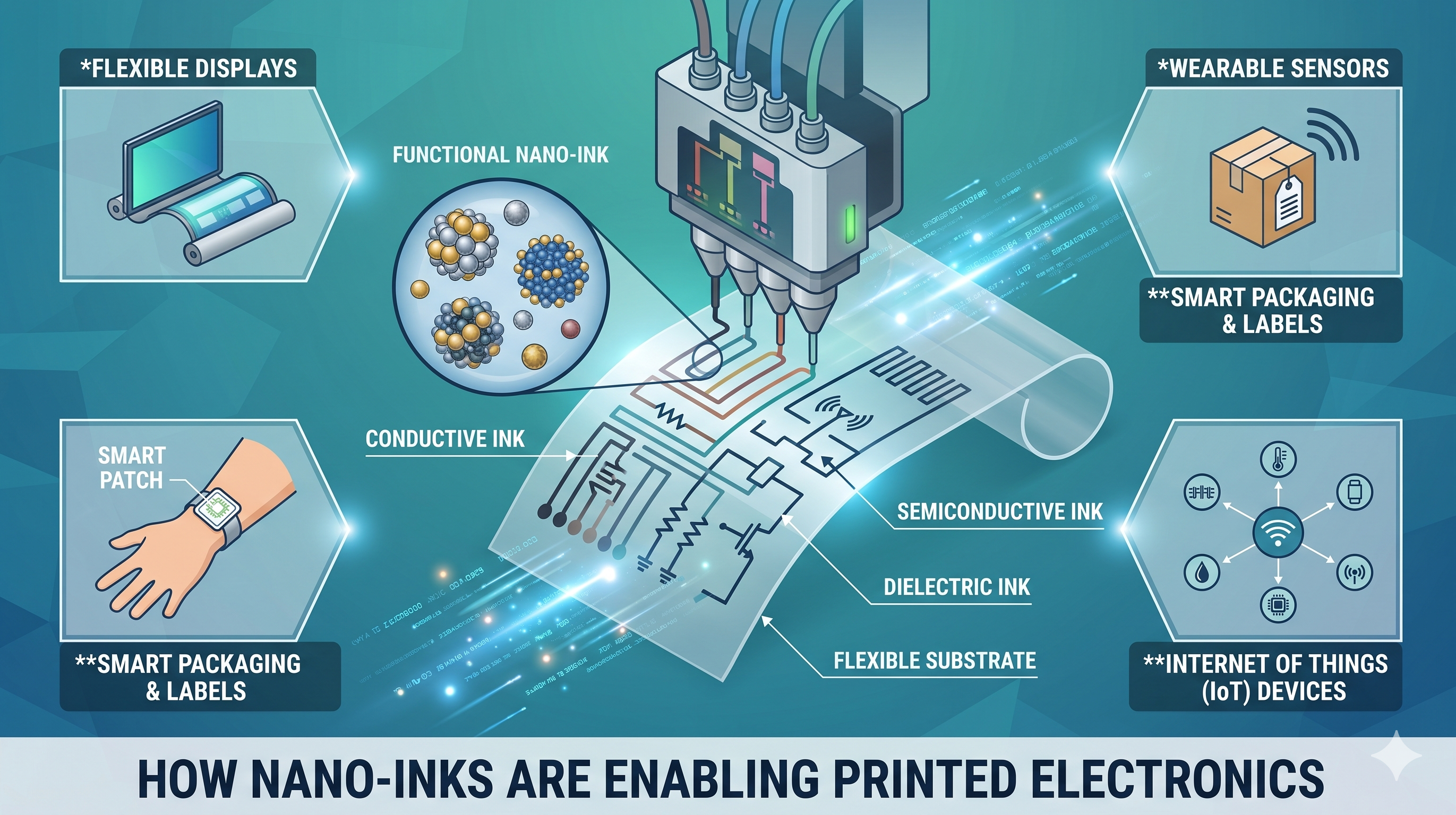
The history of electronics has traditionally been a story of “subtraction.” To make a computer chip, we start with a wafer of pure silicon and use light and chemicals to etch away everything that isn’t a circuit. This process, known as photolithography, is incredibly precise but also incredibly expensive, wasteful, and restricted to rigid, flat surfaces.
However, a fundamental shift is occurring in material science. We are moving from a “subtractive” world to an “additive” one. Instead of etching circuits, we are now printing them. Just as an office printer deposits ink on paper to form words, “Printed Electronics” uses specialized Nano-Inks to deposit functional circuits onto almost any surface—plastic, fabric, paper, and even human skin.
Nano-inks are the “secret sauce” of this revolution. By manipulating materials at the scale of atoms and molecules, we have created liquids that can conduct electricity, sense touch, and emit light. This isn’t just about making gadgets cheaper; it is about making electronics ubiquitous, flexible, and integrated into the very fabric of our lives.
Understanding the Fluid: What Exactly is a Nano-Ink?
A standard ink consists of a pigment (for color), a solvent (to keep it liquid), and a binder (to stick it to the paper). A nano-ink follows a similar blueprint, but the “pigment” is replaced by nanoparticles that possess electrical or optical properties.
At the heart of a nano-ink are functional particles, typically measuring between 1 and 100 nanometers. At this scale, materials behave differently. For instance, silver nanoparticles have a much lower melting point than bulk silver. This allows us to “sinter” or fuse the ink into a solid, conductive path at temperatures low enough that they won’t melt a plastic bottle or a piece of paper.
Nano-inks generally fall into three categories:
-
Conductive Inks: Typically made of silver, copper, or gold nanoparticles. These form the “wires” of the printed circuit.
-
Semiconductive Inks: Often based on organic polymers or metal oxides. These are used to print transistors—the “brains” that switch signals on and off.
-
Dielectric Inks: These act as insulators, preventing short circuits and allowing for the creation of capacitors.
The Materials of Choice: Silver, Copper, and Carbon
The choice of nanomaterial determines the ink’s performance, cost, and durability.
1. Silver Nanoparticles (The Industry Standard)
Silver is the king of conductive inks. It has the highest electrical conductivity of any element and is chemically stable. Because silver nano-inks can be printed with high precision and low resistance, they are used in everything from smartphone touchscreens to RFID tags. However, silver is expensive, which has pushed researchers to look for alternatives.
2. Copper Nanoparticles (The Economic Challenger)
Copper is nearly as conductive as silver but significantly cheaper. The challenge? Copper oxidizes (rusts) almost instantly when exposed to air, forming an insulating layer that kills conductivity. Current research in 2025 and 2026 has focused on “Core-Shell” nanoparticles—coating a copper core with a thin layer of silver or a protective polymer to keep the copper pure while it is being printed and cured.
3. Graphene and Carbon Nanotubes (The Flexible Frontiers)
Carbon-based nano-inks are the future of “Wearable Electronics.” Graphene is incredibly strong, transparent, and flexible. Unlike metallic inks, which can crack when folded, graphene-based inks can be bent thousands of times without losing their ability to conduct electricity. This makes them ideal for smart clothing and flexible medical patches.
Printing Technologies: From Desktop to Industrial Scale
Nano-inks are compatible with several high-speed printing methods, each with its own strengths:
-
Inkjet Printing: Offers the highest resolution. It is a “non-contact” method, meaning it can print onto delicate or uneven surfaces. It is perfect for rapid prototyping and custom medical devices.
-
Screen Printing: A rugged, high-volume method used for making solar cells, glucose test strips, and heated car seats. It can deposit thicker layers of nano-ink for higher power applications.
-
Gravure and Flexography: These are the “Formula 1” of printing, capable of producing miles of electronic circuits on rolls of plastic at speeds of hundreds of meters per minute.
Current Research (2025-2026): Sintering and Sustainability
The two biggest hurdles in printed electronics have traditionally been the “curing” process and environmental impact.
Room-Temperature Sintering
To turn a liquid ink into a solid wire, you usually need to heat it (sintering). In 2026, a major breakthrough involved Chemical Sintering Inks. These inks contain a “trigger” molecule that fuses the nanoparticles together the moment the solvent evaporates, requiring zero heat. This allows for printing electronics directly onto heat-sensitive biological tissues or thin food packaging.
“Green” and Biodegradable Inks
The electronics industry is a massive source of “e-waste.” Current research is pioneering Transient Electronics—inks made from materials like zinc or magnesium that are dissolved by water or soil over time. These allow for the creation of environmental sensors that can be scattered across a field to monitor soil health and simply dissolve after the growing season, leaving zero toxic residue.
Clinical Perspectives: Wearable Biosensors and “Smart Skin”
The most profound impact of nano-inks is seen in the medical field. Clinical studies are increasingly focusing on “Epidermal Electronics”—circuits that are as soft and thin as human skin.
1. Continuous Glucose Monitoring (CGM)
Traditional glucose monitors require a needle. New clinical trials are using printed nano-ink patches that use “Reverse Iontophoresis” to pull glucose through the skin and measure it using a printed electrochemical sensor. These patches are thin enough to be worn under clothing and provide real-time data to a smartphone.
2. Cardiac and Muscle Monitoring
Clinical research published in early 2026 showcased printed “Electronic Tattoos” made of gold and graphene nano-inks. These sensors adhere directly to the chest or limbs to provide long-term ECG (heart) and EMG (muscle) data with higher signal quality than traditional gel-based electrodes, which often cause skin irritation during long-term use.
3. Smart Bandages
Researchers are developing bandages with printed nano-inks that can detect the specific pH and temperature of a wound. If the sensor detects a spike in temperature (a sign of infection), it can trigger the release of an antibiotic stored in a printed polymer layer.
Advantage vs. Risk Assessment
As with any disruptive technology, printed electronics come with a balance of benefits and concerns.
The Advantages:
-
Cost Efficiency: Eliminates the need for cleanrooms and vacuum chambers. You only use the material you print (additive), reducing waste by up to 90%.
-
Form Factor: Electronics can finally be thin, light, and flexible.
-
Speed: Allows for “Mass Customization.” You can print a unique medical sensor for a specific patient in minutes.
-
Integration: Enables the “Internet of Everything” (IoE), where every milk carton or medication bottle can have a low-cost printed sensor.
The Risks and Challenges:
-
Conductivity Limits: Printed silver is still roughly 10 times less conductive than bulk copper wire. This limits printed electronics to low-power applications for now.
-
Environmental Toxicity: While “green” inks are being developed, many current nano-inks use silver or carbon nanotubes, which can be toxic if they leach into the water supply.
-
Durability: Printed circuits can be sensitive to humidity and oxygen. Without proper “encapsulation” (protective coating), a printed sensor might only last a few months.
-
Regulatory Hurdles: For medical applications, ensuring the “biocompatibility” of nanoparticles is a slow and rigorous clinical process.
The Road Ahead: The Invisible Computer
By 2030, the “black box” of electronics will disappear. Instead of carrying a rigid phone, our devices will be integrated into our clothes, our windows, and our walls. We will see “Smart Packaging” that tells us exactly when food is spoiling and “Smart Infrastructure” where bridges use printed nano-inks to sense structural cracks before they become dangerous.
The transition from silicon wafers to nano-inks is more than a manufacturing change; it is a democratization of technology. It allows for the local production of electronics and opens the door to a world where intelligence is woven into every object we touch.
Conclusion
Nano-inks are the bridge between the digital and physical worlds. By turning functional materials into printable fluids, we have unlocked a level of design freedom that was previously science fiction. Whether it is through the clinical success of wearable health patches or the industrial efficiency of printed solar cells, the impact of nano-inks is undeniable. As we refine these materials to be more conductive, more stable, and more sustainable, the “inkjet” may become the most powerful tool in the electronics engineer’s arsenal.