
Recently added item(s)
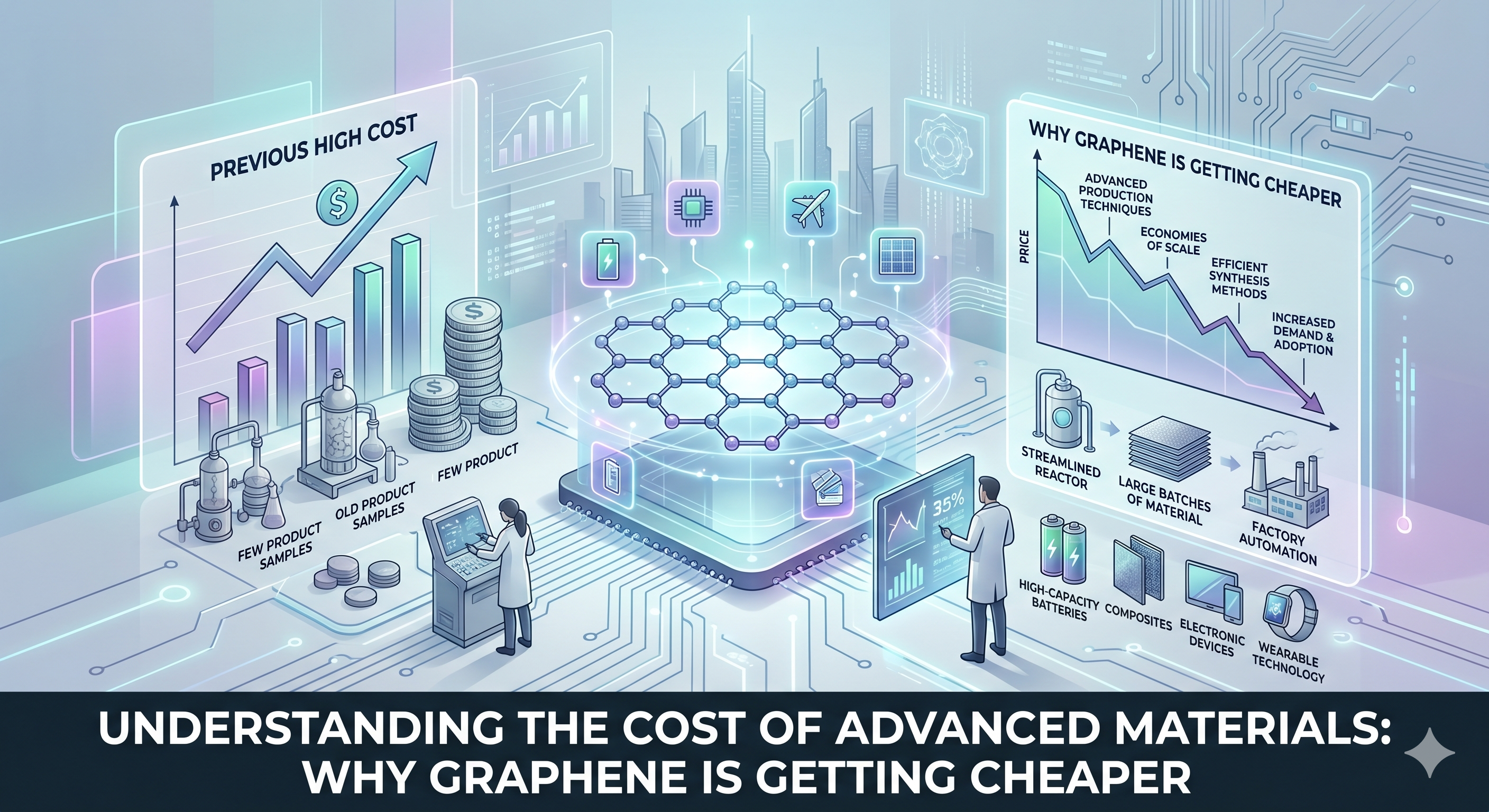
It is often hailed as the “wonder material” of the 21st century. Isolated for the first time in 2004 at the University of Manchester—a breakthrough that earned the Nobel Prize in Physics—graphene promised to revolutionize everything from electricity to medicine. It is a single layer of carbon atoms arranged in a hexagonal lattice, a monolayer structure that makes it the thinnest material known to humanity, yet it is about 200 times stronger than steel, lighter than paper, and possesses extraordinary electrical and thermal conductivity.
For nearly two decades, however, a paradox defined graphene: while its theoretical capabilities were unparalleled, its price tag made it a laboratory curiosity. In the early 2010s, a theoretical gram of single-layer pristine graphene could cost tens of thousands or even hundreds of thousands of dollars to produce in usable flakes. Industrial applications were impossible.
Today, on May 8, 2026, the landscape has fundamentally shifted. The paradox is dissolving. We are witnessing the maturation of the graphene market, where economies of scale, innovative manufacturing processes, and the utilization of alternative feedstocks have combined to drive prices down by magnitudes. Graphene is transforming from a prohibitive luxury ingredient into a commercially viable additive.
To understand why this change is happening, we must first understand how graphene is made and why early manufacturing was so expensive.
Deconstructing the Cost: How Graphene is Made
A key misconception about graphene is that “all graphene is created equal.” When people talk about graphene becoming cheaper, they are often referring to specific grades or forms of the material, which serve different industrial needs.
Generally, graphene is categorized into four main types:
-
Pristine Monolayer Graphene: The high-quality, continuous, single-sheet graphene desired for advanced electronics and transistors. This remains the most expensive grade.
-
Chemical Vapor Deposition (CVD) Graphene Films: Films grown on metal substrates. They offer excellent quality for optoelectronics but have traditionally faced high costs due to energy consumption and the difficulty of “transferring” the film without damaging it.
-
Graphene Oxide (GO) and reduced Graphene Oxide (rGO): Chemically modified forms. GO is soluble in water, making it easier to handle for coatings and composites, but the chemical processing required to create it, and then “reduce” it to restore conductivity, has historically been labor-intensive and environmentally costly.
-
Graphene Nanoplatelets (GNPs): Flakes of multi-layer graphene (typically 2 to 10 layers). These are easiest to scale for industrial volume and are the main driver of the current cost reduction wave.
The classic manufacturing methods are split into two philosophies: “top-down” and “bottom-up.”
The “Top-Down” Expense: Peeling the Onion
“Top-down” approaches involve taking bulk graphite (the carbon stuff in your pencil) and exfoliating, or peeling, layers away until you get down to monolayers or few-layers.
For a long time, the dominant “top-down” method for bulk production was a variant of the Hummers’ Method, developed in 1958. This method uses harsh oxidizing agents like sulfuric acid, sodium nitrate, and potassium permanganate to turn graphite into graphite oxide, which then easily exfoliates into GO.
While effective, this method is fundamentally expensive because:
-
Reagent Cost: It requires large quantities of expensive and hazardous chemicals.
-
Complexity: The process involves multiple heating, cooling, washing, and filtration steps.
-
Environmental Handling: Neutralizing and disposing of the hazardous chemical waste adds significant overhead.
The “Bottom-Up” Barrier: Building Atom by Atom
“Bottom-up” approaches involve assembling carbon atoms into the graphene lattice from a carbon gas precursor, typically via CVD. This method produces the highest-quality large-area sheets.
However, CVD faced high barriers to cost reduction:
-
Substrate Cost: Graphene grows best on specific, polished metal catalytic substrates, like copper or nickel, which can be expensive.
-
Energy Consumption: The process requires extremely high temperatures (often exceeding 1000^\circ\text{C}).
-
The Transfer Problem: Getting the graphene off the metal substrate and onto a desired surface (like a silicon wafer for computer chips) historically damaged the sheet, requiring expensive, slow, and low-yield specialized techniques.
The Drivers of Cheap Graphene: Why the Price is Plummeting Now
As we sit here in 2026, the price of graphene nanoplatelets has dropped from the early 100+/gram levels to competitive commodity levels, ranging from 50 to 500 per kilogram depending on grade and purity. High-quality CVD films have also seen their costs drop by over 90% per square centimeter since the early 2020s.
This dramatic reduction is not due to a single breakthrough, but rather the convergence of three major factors.
1. The Scaling of Sustainable “Top-Down” Exfoliation
The first factor is pure economies of scale. Major graphene manufacturers around the world have transitioned from small batch processing to continuous, tonnage-scale automated plants. Operating at 100+ ton annual capacity has allowed companies to reduce unit costs by 75–80%.
Furthermore, older chemical methods have been refined or replaced by greener, simplified mechanical and liquid-phase exfoliation (LPE) techniques. These methods use high-shear mixing, ultrasonication, or electrochemical forces in sustainable solvents (including water in some specialized processes) to shear graphene flakes off graphite without needing harsh oxidizing reagents. This simplifies the process, increases throughput, and removes the massive expense of hazardous waste management.
2. The Breakthrough of Waste Carbon Feedstocks: Flash Graphene
Perhaps the most disruptive technological leap in the cost discussion is the advent of techniques like Flash Joule Heating (FJH). Championed initially by Rice University, FJH allows for the conversion of virtually any cheap or waste carbon feedstock—including plastic waste, municipal solid waste, biomass, rubber tires, and coal—directly into high-quality graphene flakes.
The process is remarkably efficient:
-
Feedstock Valorization: It turns landfill-bound trash, which usually has a negative cost (you are paid to take it), into a valuable asset.
-
Low Energy Cost: Because the heating is applied in massive, instantaneous “flashes” (reaching over 3000\text{K} in milliseconds), the total energy consumed to produce a gram of “Flash Graphene” is a fraction of that used by conventional bulk methods (approximately 7.2\text{ kJ/g}).
This method has decoupled graphene pricing from the price of premium graphite, transforming graphene manufacturing into a potential component of waste valorization and circular economy systems.
3. Optimization of CVD Transfer and Substrates
In the CVD sector, the high costs of production have been addressed through innovative engineering rather than a shift in feedstock.
Significant developments leading up to 2026 include:
-
Substrate Reuse: Optimized processes now allow for the non-destructive removal of graphene films, enabling the metal catalytic substrate to be reused hundreds of times, amortizing its initial cost to nearly zero.
-
Improved Transfer Techniques: Optimized roll-to-roll transfer systems use dry, specialized polymers to lift and place graphene films onto substrates without using harsh chemical etching, dramatically increasing the throughput and yield of continuous high-quality films for the electronics industry.
Graphene Goes to Work: Real-World Applications Fueling Demand
Cost reduction has created a feedback loop: as graphene gets cheaper, its adoption rate in high-volume industries increases, which further drives down costs due to increased production demand.
Concrete and Construction: Lowering Carbon Footprints
One of the largest consumers of bulk graphene nanoplatelets today is the construction industry. Concrete is the most used man-made material on Earth, and cement production is responsible for around 8% of global \text{CO}_2 emissions.
The addition of just 0.03% by weight of specialized graphene oxide or reduced graphene oxide to concrete can:
-
Increase compressive strength by 25%.
-
Decrease water permeability by a factor of 4.
-
Significantly improve the material’s durability and resistance to cracking.
Crucially, because graphene makes concrete stronger, construction firms can achieve the required design strength using significantly less concrete, potentially reducing global cement consumption by billions of tons annually and offering a cost-effective path to greener infrastructure.
Anti-Corrosion Coatings and Paints
Another massive industrial market is protective coatings. Conventional epoxy coatings protect assets (like ships, pipelines, or steel bridges) for 5 to 7 years. Because graphene is impermeable to all gases and liquids, it acts as the ultimate barrier coating.
Graphene-enhanced formulations are now extending asset lifecycles to 12 to 15 years. This drastic reduction in maintenance cycles (a 60% reduction in maintenance costs) makes graphene-enhanced paints an economical choice, even if the paint itself is slightly more expensive per liter.
Graphene in Medicine: The Frontier of Clinical Application
Perhaps the most strictly regulated and biologically sensitive area for graphene adoption is medicine. Here, the requirements are not for “cheap bulk” material, but for extremely high-purity, standardized, functionalized, and biocompatible graphene grades.
While widespread routine clinical use for many therapies is still decades away, by May 2026, several graphene biomedical products have reached advanced clinical trial stages (pre-clinical or Phase I).
Biosensors and Diagnostic Trials
Because of its extraordinary electrical properties, graphene is the ideal material for ultrasensitive, real-time diagnostic sensors. The high surface area allows for the binding of large numbers of bioreceptors (like antibodies or DNA). A single antigen binding event significantly alters the electrical resistance of the graphene sheet, offering near-instant detection. Clinical trials have been underway for devices detecting COVID-19 biomarkers, cancer cells, and specific proteins associated with neurological disease. These trials are currently testing the reliability, specificity, and shelf-life of these disposable sensor chips in clinical settings.
Neural Interfaces and Advanced Brain Implants
Graphene’s high conductivity, combined with its flexibility and potential for functionalization to reduce immune rejection, has positioned it as the future material for neuroprosthetics. Metal electrodes are stiff and can cause scarring when implanted into the soft brain tissue. Flexible graphene electrodes offer a stable, long-term interface. The Graphene Flagship initiative and private neurotech ventures have reached advanced pre-clinical stages with flexible neural probes that can record brain activity with significantly higher resolution than traditional technologies and, critically, can stimulate brain tissue with finer control. These devices offer clinical promise for treatments for Parkinson’s disease, epilepsy, and spinal cord injuries.
Advantages and Risks Assessment: The Two Sides of the Monolayer
The widespread commercialization of graphene is a transformative development, but it is accompanied by essential safety and sustainability assessments.
Advantages: Efficiency and Performance
-
Multifunctionality: Graphene enables “smart” materials where a single addition consolidates performance requirements (e.g., lightweight composites that are also electrically conductive for EMI shielding, and thermally conductive for heat dissipation).
-
Durability and Lifecycle Extension: By increasing the lifespan of assets (concrete, metal infrastructure) and the durability of consumer products (batteries, automotive components), graphene can reduce global consumption and waste.
-
New Functionality: Graphene enables entirely new device categories, such as flexible, wearable electronics and instant biosensors.
Risks: Safety and Standardization
-
Toxicity of Nanopowders: The primary safety concern is the inhalation toxicity of graphene powders. Like all nanoparticles, particularly those that are thin and rigid, high concentrations of inhaled graphene particles can cause lung inflammation or scarring, a concern often compared to asbestos (though studies are nuanced). Manufacturing processes must prioritize the handling of graphene in suspended liquid or functionalized flake form rather than dry powder, and factory workers must have rigorous PPE protocols.
-
Environmental Impact of Chemical Solvents: While older methods like Hummer’s Method are being replaced, some current exfoliation processes still rely on toxic solvents like NMP (N-Methyl-2-pyrrolidone). The continuous shift towards green chemistry and water-based solvents is critical for the industry’s long-term sustainability.
-
Lack of Affordable Standardization: A remaining industry weakness is the lack of adopted international standards for what truly constitutes different grades of “graphene Related Materials” (GRMs). Statistical assessment of entire batches requires expensive, sophisticated equipment (like TEM, Raman, AFM). Standardized, industry-affordable quality control tools are needed to ensure material consistency for end-users.
Conclusion: The Era of the Industrial Carbon
As of May 2026, the graphene paradox has resolved. The question is no longer “When will graphene become affordable?” but “Which grade of industrial carbon best serves this application?” The convergence of economies of scale, waste-valorizing manufacturing, and standardized sustainable processes has brought graphene to the commercial tipping point.
Pure lab curiosity has matured into a powerful industrial ingredient. Its properties, once only achievable in micro-flakes on “scotch tape,” are now enabling stronger bridges, longer-lasting ships, and smarter diagnostics. The era of prohibitive pricing is over; the era of industrial-scale graphene integration has arrived.