Recently added item(s)
1. Introduction: The Need to See the Invisible
In the world of nanotechnology, seeing is not just believing—it is the foundation of science. When we develop a bio-compatible coating for an implant or a carbon nanotube scaffold for regenerative medicine, we are working with structures that are thousands of times smaller than the width of a human hair. At this scale, the laws of classical physics fade, and the unique properties of matter emerge.
But how do we know if we have actually built what we intended? How do we measure the diameter of a nanotube or the crystal purity of a nanoparticle? This is where Nanomaterial Characterization comes in. Using specialized tools like Scanning Electron Microscopy (SEM), Transmission Electron Microscopy (TEM), and X-Ray Diffraction (XRD), scientists can “see” atoms, map surfaces, and identify chemical structures. This article provides a comprehensive guide to these three pillars of nanotechnology.
2. Scanning Electron Microscopy (SEM): The High-Resolution Map
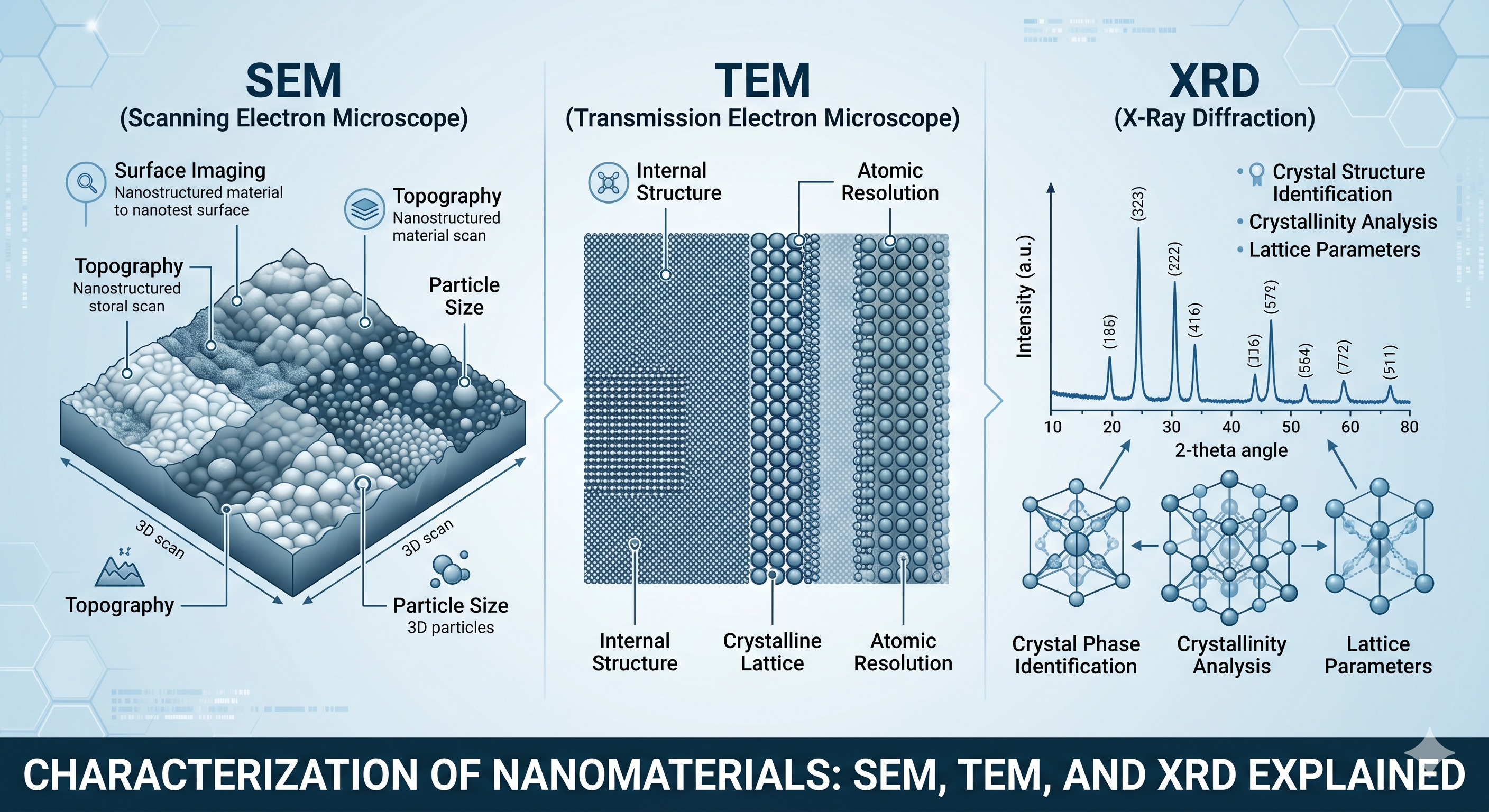
If you want to see the “landscape” of a nanomaterial, SEM is the tool of choice. Traditional microscopes use light, but light has a physical limit (wavelength) that prevents it from seeing anything smaller than about 200 nanometers. SEM overcomes this by using a beam of electrons instead of light.
How It Works:
An electron gun fires a beam at the sample. As the beam scans the surface, it knocks “secondary electrons” off the material. A detector captures these electrons and converts them into a 3D-like image of the surface.
-
Clinical Application: SEM is vital for inspecting medical implants. It allows researchers to see how well bone cells are attaching to a bio-compatible coating. If the surface is too smooth, cells won’t stick; if it’s too rough, it might cause inflammation. SEM provides the visual proof needed to optimize these surfaces.
3. Transmission Electron Microscopy (TEM): Seeing Through Atoms
While SEM looks at the surface, TEM looks through the material. It is the most powerful imaging tool in a scientist’s arsenal, capable of reaching magnifications of several million times—enough to see individual columns of atoms.
How It Works:
TEM works similarly to a slide projector. A high-energy electron beam is passed through an incredibly thin slice of the sample (often less than 100 nanometers thick). The electrons that pass through are gathered to form an image that reveals the internal structure, density, and even the “defects” in a crystal lattice.
-
Research Focus: TEM is the gold standard for characterizing Carbon Nanotubes (CNTs). It is the only way to verify if a nanotube is single-walled or multi-walled and to check for residual catalyst metals that might be toxic to human cells.
4. X-Ray Diffraction (XRD): The Chemical Fingerprint
SEM and TEM give us pictures, but XRD gives us the “ID card” of a material. It doesn’t produce an image; instead, it produces a graph (a diffractogram) that tells us the exact crystalline phases present in a sample.
How It Works:
When X-rays hit a crystalline nanomaterial, they are scattered (diffracted) in specific patterns based on the arrangement of atoms. By measuring the angles and intensities of these scattered rays, scientists can calculate the distance between atoms and identify the substance.
-
Global Regulatory View: XRD is essential for the safety of nanomaterials in healthcare. Regulators like the FDA use XRD data to ensure that a drug-delivery nanoparticle is pure and hasn’t changed its chemical structure during manufacturing, which could alter its toxicity or effectiveness.
5. Direct Comparison: SEM vs. TEM vs. XRD
To understand which tool is best for a specific job, we must compare their capabilities.
| Feature | SEM (Scanning) | TEM (Transmission) | XRD (Diffraction) |
| Primary Output | 3D Surface Image | 2D Internal Image | Atomic Structure Graph |
| Resolution | 1 – 20 nanometers | Sub-nanometer (Atomic) | N/A (Atomic Distances) |
| Sample Prep | Easy (Surface coating) | Very Difficult (Ultra-thin) | Moderate (Powder form) |
| Main Use | Morphology & Topography | Internal Defects & Atoms | Purity & Crystallinity |
6. Recent Trends: In-Situ and Cryo-Characterization
Modern research is moving beyond looking at “dead,” dry samples.
-
Cryo-TEM: This technique involves freezing samples (like mRNA vaccines or soft tissue scaffolds) so quickly that the water doesn’t form ice crystals. This allows scientists to see nanomaterials in their natural, “wet” biological state.
-
In-Situ SEM: Researchers are now performing “miniature experiments” inside the microscope. They can heat an implant coating or apply an electrical current to a Brain-Machine Interface sensor and watch in real-time how the nanomaterial reacts.
7. Advantage vs. Risk Assessment: The Cost of Precision
Characterization is the most expensive part of nanotechnology development.
| Advantage | Clinical Benefit | Risk / Challenge | Technical Burden |
| Quality Control | Ensures every implant is safe for the patient. | Artifacts | High-energy electron beams can sometimes damage or melt delicate biological samples. |
| Mechanism Discovery | Helps us understand why a rapid pathogen sensor works. | Cost | These machines cost millions of dollars and require specialized facilities to operate. |
| Standardization |
Provides the data needed for global regulatory approval.
|
Representation | TEM looks at a tiny area; researchers must ensure that one image represents the whole batch. |
8. The Future: Integrated Characterization
The future of nanotechnology is “Multimodal Characterization.” New machines are being built that combine SEM, TEM, and XRD into a single workflow. Imagine a system where you can scan the surface of a lateral flow assay, zoom in to see the individual gold nanoparticles, and verify their crystal purity—all within an hour. This speed will be essential as we move toward personalized medicine and 3D-printed bio-implants.
9. Conclusion: The Eyes of the Nano-Scientist
Without SEM, TEM, and XRD, the field of nanotechnology would be blind. These tools allow us to bridge the gap between a theoretical design and a life-saving medical product. Whether we are checking the conductivity of a neural probe or the antimicrobial surface of a prosthetic, characterization provides the evidence that makes nanomedicine both possible and safe.
As these technologies become more accessible and automated, they will continue to drive the “nano-revolution,” ensuring that the invisible tools of the future are built with the highest levels of precision and care.