
Recently added item(s)
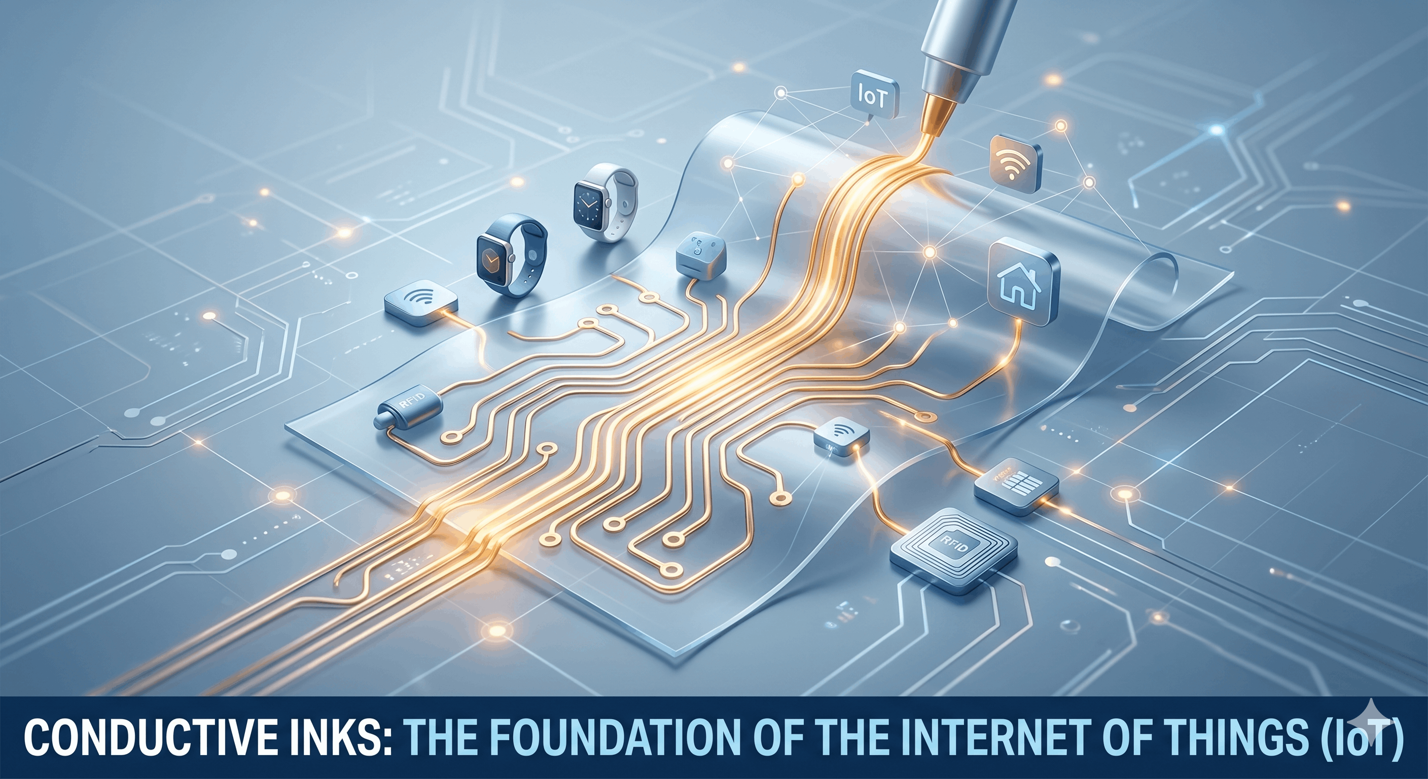
The Internet of Things (IoT) is no longer a futuristic concept; it is the reality of our connected world. From smartwatches tracking our heartbeats to industrial sensors optimizing supply chains, billions of devices are now communicating wirelessly. At the heart of this revolution lies a critical, yet often invisible, technology: conductive inks. These specialized materials are transforming traditional, rigid electronics into flexible, stretchable, and lightweight systems, effectively serving as the foundational circuitry upon which the sprawling ecosystem of IoT is built.
Traditional electronics rely on rigid Printed Circuit Boards (PCBs) made of copper laminated onto fiberglass. While effective, they are bulky, expensive to manufacture in small batches, and cannot be applied to curved or flexible surfaces. Conductive inks solve these problems by enabling printed electronics. This process is akin to printing a document, but instead of decorative colors, the “printer” deposits functional electronic materials—conductive, resistive, or semiconductive traces—onto diverse substrates like plastic films, paper, textiles, and even human skin.
This article delves into the science of conductive inks, their central role in the IoT rollout, advancements in recent research, and a critical analysis of their benefits and associated risks.
1. What Are Conductive Inks? The Science Beneath the Surface
At its core, a conductive ink is a substance that allows electricity to flow after it has been applied and “cured” (dried or heated). They are fundamentally composed of three main components, each vital to the final ink’s performance:
-
Conductive Fillers: This is the functional element that carries the electric current. Most common fillers are metallic nanoparticles, such as silver, copper, or gold. Carbon-based materials, including graphite and graphene, and conductive polymers like PEDOT:PSS are also widely used.
-
Binder (Polymer Matrix): This ingredient acts as the “glue” that holds the conductive particles together and ensures they adhere firmly to the substrate. The choice of binder determines the flexibility and mechanical strength of the final circuit.
-
Solvent/Vehicle: This liquid component allows the ink to remain in a liquid state for printing. It must evaporate quickly and cleanly during the curing process, leaving behind a solid, conductive trace.
The Mechanism of Conductivity
For electricity to flow, the conductive filler particles must form a continuous pathway—a phenomenon known as percolation. When the ink is first printed, the particles are separated by solvent. During curing, the solvent evaporates, bringing the particles into physical contact. The binder then solidifies, trapping them in this network, creating a highway for electrons.
Common Printing Techniques
Conductive inks are compatible with various established printing technologies, allowing for scalable manufacturing:
-
Screen Printing: Best for thick traces and mass production (e.g., RFID tags).
-
Inkjet Printing: Enables precise, high-resolution deposition for prototyping or customized circuits.
-
Gravure and Flexography: High-speed roll-to-roll (R2R) processes for very large-scale manufacturing.
2. Why Conductive Inks are Crucial for the IoT Ecosystem
The defining characteristic of IoT devices is their ubiquity. To be everywhere, they must be unobtrusive, cheap, and conformable. Conductive inks meet these exact demands, making them the enabler for several key IoT application areas:
A. Flexible and Wearable Electronics
Traditional rigid electronics are incompatible with human comfort. Conductive inks allow for the creation of wearable health monitors—smart patches that stick directly to skin to measure ECG, temperature, or hydration levels. These devices must stretch and bend with movement without breaking the circuit. Research is now focusing on self-healing inks that can repair microscopic tears caused by mechanical stress.
B. Smart Packaging and Logistics
One of the earliest and most impactful IoT applications is asset tracking using Radio Frequency Identification (RFID) and Near Field Communication (NFC). Conductive inks are now used to print RFID antennas directly onto cardboard boxes, product labels, or even pharmaceutical packaging. This makes “item-level tagging” financially viable for everyday consumer goods, enabling real-time inventory management and anti-counterfeiting measures throughout the supply chain.
C. Large-Scale Sensor Networks
IoT relies on collecting data from vast numbers of sensors. Printed electronics allow sensors (e.g., temperature, humidity, gas) to be manufactured in large batches at a fraction of the cost of traditional semiconductor fabrication. They can be integrated into buildings (smart walls), textiles (smart clothing), or environmental monitoring stations.
3. Current Advancements and Recent Research
The field of conductive inks is moving rapidly, driven by the need for better performance, lower cost, and greater environmental sustainability.
Graphene and Carbon-Based Inks
While silver remains the dominant material due to its high conductivity, its volatile price is a significant barrier to massive IoT rollout. Recent research has focused heavily on graphene, a single layer of carbon atoms with extraordinary electrical properties. While earlier graphene inks struggled with low conductivity, new formulation techniques and low-temperature curing methods have drastically improved their performance, making them a viable, low-cost alternative for RFID antennas and sensors.
Biodegradable and Sustainable Inks
With billions of new IoT devices poised to enter the market, electronic waste (e-waste) is a growing concern. Scientists are developing “green electronics” by formulating conductive inks that use bio-based binders (like starch or lignin) and are printed onto biodegradable substrates like cellulose nanopaper. Some research even explores biogenic silver particles synthesized using microorganisms to reduce the environmental footprint of nanoparticle production.
Clinical Studies and Biomedical Applications
Conductive inks are moving from lab prototypes to clinical validation. Recent studies have demonstrated the efficacy of printed sensor patches for monitoring parameters in a hospital setting. For example, some clinical trials are testing fully water-soluble, self-doped conductive polymer inks printed directly onto clothing for non-invasive monitoring of respiratory rates. These printed electrodes show performance comparable to traditional medical-grade electrodes but offer vastly superior patient comfort.
4. Advantages vs. Risks: A Critical Evaluation
While conductive inks offer transformative potential, their widespread adoption requires a balance of benefits and potential pitfalls.
Advantages of Conductive Inks
-
Form Factor Flexibility: Enables lightweight, flexible, and conformable devices that traditional PCBs cannot match.
-
Cost-Effectiveness at Scale: Utilizes high-speed printing processes (like roll-to-roll) that drastically reduce manufacturing costs for high-volume, simple components like antennas and basic sensors.
-
Additive Manufacturing: Unlike traditional PCB milling, which subtracts material from a sheet, printing is an additive process. It places material only where needed, reducing waste.
-
Rapid Prototyping: Allows developers to iterate electronic designs rapidly using standard printer technology before committing to mass production.
-
Biocompatibility: Many formulations, particularly carbon-based inks, are inherently biocompatible, enabling safe, long-term contact with human skin.
Risks and Challenges
-
Lower Electrical Performance: Even the best silver inks cannot match the conductivity of bulk copper found in traditional PCBs. They are unsuitable for high-power or ultra-high-speed data transmission.
-
Durability and Reliability: Printed traces are more susceptible to mechanical failure from repeated bending, twisting, or environmental factors (humidity, temperature changes). Some metallic nanoparticles can oxidize over time, degrading performance.
-
Complex Processing: To achieve optimal conductivity, many inks require high-temperature curing, which can damage cheap flexible substrates like plastics or paper. New “flash” curing techniques are addressing this but add complexity.
-
Material Costs (for precious metals): Silver-based inks, though the gold standard for performance, remain expensive, impacting the marginal cost of cheap IoT devices.
-
Environmental Toxins: While carbon inks are green, many metallic nanoparticle formulations use toxic solvents or binders that pose disposal challenges if not managed properly. Silver itself can be toxic to aquatic life.
5. The Road Ahead: The Future of IoT Foundations
Conductive inks are not just a technological curiosity; they are the architectural prerequisite for the billions-of-devices reality the IoT promises. They have bridged the gap between functional electronics and the malleable materials of our everyday environment—fabrics, paper, and skin.
As research continues to lower the cost of functional carbon-based inks, improve the reliability of printed circuits, and develop truly circular economy models for biodegradable e-waste, the impact of conductive inks will only intensify. They are the ink writing the first draft of our hyper-connected future, turning static objects into active, communicative nodes on the global web of things.