
Recently added item(s)
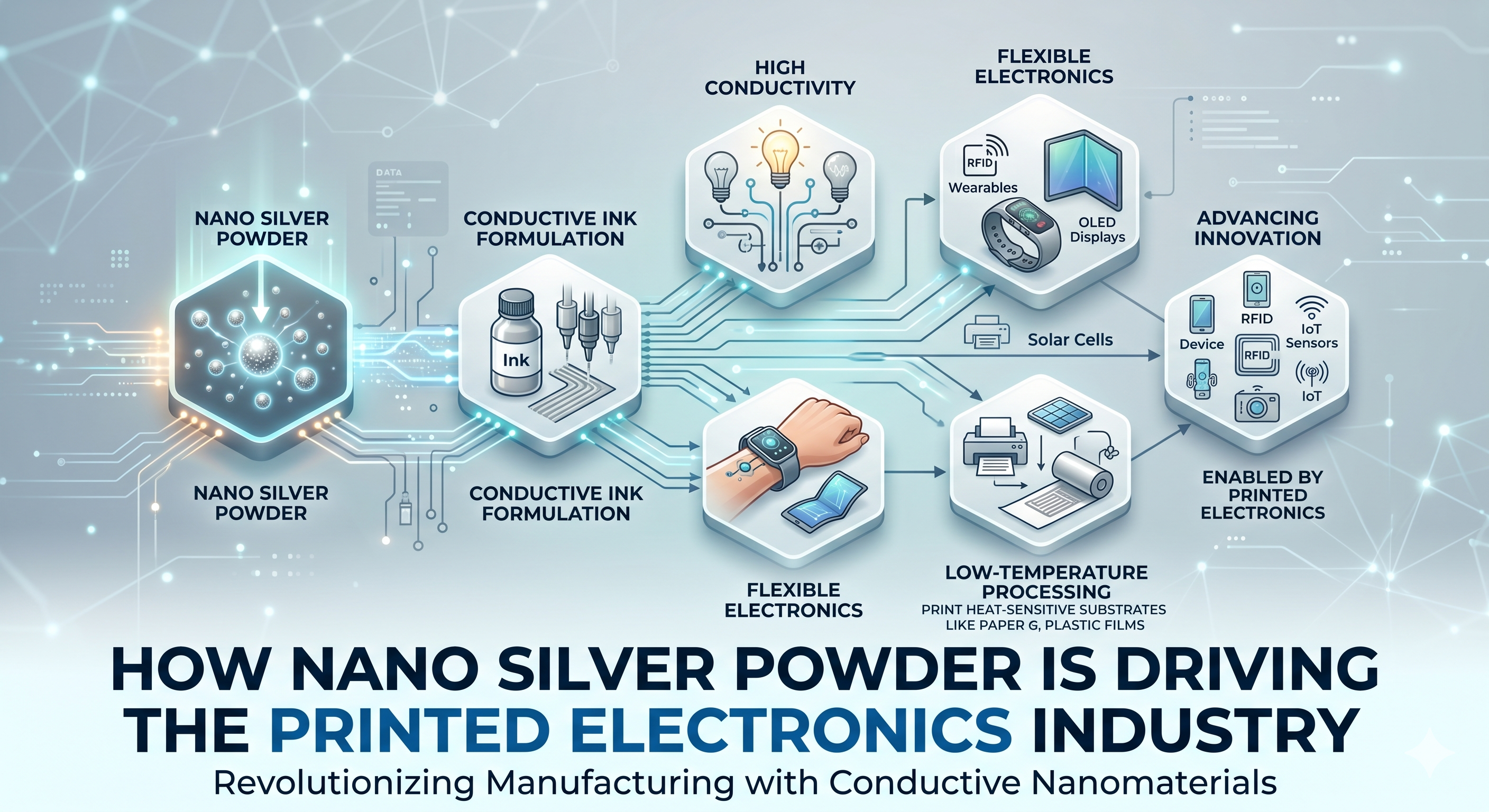
The electronics industry is undergoing a silent but profound transformation. We are moving away from rigid, silicon-based circuits enclosed in bulky plastic shells and towards a future where devices are flexible, transparent, and ubiquitous. The driving force behind this revolution is Printed Electronics (PE), a technology that allows electronic circuits and components to be printed onto various surfaces using additive manufacturing methods, just like ink on paper. And the critical ingredient making this “printed future” a reality is a microscopic marvel: Nano Silver Powder.
While traditional conductive inks rely on micro-sized particles or metal-organic compounds, nano silver powder is proving to be the indispensable material that unlocks the full potential of printed electronics. Its unique physical, chemical, and optical properties at the nanoscale are overcoming previous bottlenecks, enabling new applications, and reshaping the way we interact with technology. This article will delve into the science of nano silver powder, explore its key roles in driving PE growth, assess its advantages and risks, and showcase current research pushing the boundaries of this exciting field.
The Scale of Change: Why Nanoparticles Matter
To understand why nano silver is so critical, we must first look at the difference between “bulk” materials (those we can see and touch) and “nanomaterials.” A nanoparticle typically has at least one dimension less than 100 nanometers (nm). For context, a strand of human hair is about 80,000 nm thick.
When a metal like silver is reduced to this scale, its properties change dramatically. Two primary effects take over: an immensely increased surface-area-to-volume ratio and quantum mechanical phenomena.
For nano silver powder, the most significant advantage is its lowered melting and sintering temperature. Bulk silver melts at 961.8 °C. For many flexible substrates used in printed electronics, such as common plastics like polyethylene terephthalate (PET) and polyethylene naphthalate (PEN), or even paper, such high temperatures would destroy the material. Nano silver, however, can be engineered to “sinter” (where particles fuse without melting) at temperatures far below 200 °C, and in some cases, even under 100 °C. This happens because a larger percentage of atoms are on the surface, requiring less energy to break free and begin binding with neighbors. This critical property enables the creation of high-conductivity patterns directly onto low-cost, heat-sensitive materials. Furthermore, nano silver particles demonstrate exceptional conductivity due to efficient electron percolation across the formed metal networks.
The Printed Electronics Revolution: A Paradigm Shift
Traditional electronics manufacturing is a complex, subtractive process involving photolithography, multiple washing stages, and chemical etching, often resulting in significant material waste. Printed electronics, by contrast, is an additive process. Conductive inks are deposited only where needed using high-throughput methods like screen printing, gravure, flexography, and inkjet printing.
The benefits are clear: reduced material consumption, faster production speeds, large-area manufacturing, and importantly, flexibility. This allows electronic functions to be integrated into clothing, medical bandages, architectural surfaces, and unconventional forms. However, the bottleneck for widespread adoption has always been the conductive ink. The performance and reliability of the electronic devices hinge entirely on the ability to print stable, highly conductive tracks with fine resolution. Nano silver powder has emerged as the clear winner, surpassing other candidates like carbon-based materials or alternative metals, and enabling the rapid acceleration of the printed electronics market.
Driving the Growth: Key Applications Enriched by Nano Silver
The impact of nano silver powder is best observed across a wide spectrum of rapidly expanding printed electronic applications:
Flexible Displays and Touchscreens
The future of smartphone and display technology lies in flexibility and unbreakability. Traditional transparent conductive oxides, such as Indium Tin Oxide (ITO), dominate the rigid screen market, but are brittle and prone to cracking under bending. Nano silver powder enables the printing of fine, transparent silver mesh or grid structures. These printed electrodes offer excellent transparency and lower sheet resistance than ITO, combined with the mechanical robustness required for foldable phones and stretchable screens. Current research focuses on maximizing optical clarity while minimizing visibility of the silver pattern.
Solar Cells
Printed electronics methods are increasingly used to manufacture low-cost solar cells, particularly organic photovoltaics (OPV) and perovskite solar cells. Highly conductive silver inks are printed for busbars and contact fingers on the cell surfaces, efficiently collecting generated electricity. Nano silver inks can be optimized to achieve precise grid resolutions, reducing shading of the active cell area while maintaining high conductivity, thus boosting overall cell efficiency. The ability to print on flexible foils also opens new installation possibilities, such as integration into windows or curved surfaces.
RFID and NFC Tags
Radio-Frequency Identification (RFID) and Near Field Communication (NFC) are critical for logistics, inventory management, and smart packaging. These tags require small antennas to communicate. Traditionally etched from metal foil, printed nano silver antennas offer a significant cost advantage. High-speed printing methods can produce thousands of tags per minute directly onto paper or plastic labels. The fine particle size of nano silver powder ensures uniform conductivity in intricate antenna designs, maximizing range and reliability even for complex geometries.
Sensors and Wearable Devices
The field of printed sensors is exploding, enabling innovations in medical diagnostics, environmental monitoring, and connected objects (IoT). Printed bio-sensors can monitor physiological indicators from sweat or saliva, while environmental sensors can detect pollutants. The extreme surface sensitivity of nano silver can be leveraged to create highly sensitive sensors. Furthermore, printed electrodes and circuits integrated into textiles or thin skins are essential for medical monitoring systems and smart garments, providing non-intrusive and robust performance over long durations. Research is focused on making these sensors stretchable, durable, and capable of wireless data transmission.
Printed Antennas
As 5G networks expand and the Internet of Things (IoT) grows, the demand for integrated, low-cost antennas in devices increases. Antennas for wearables, IoT nodes, and automotive systems can be printed onto surfaces or curved enclosures. Nano silver powder allows for the direct printing of antennas with complex designs on flexible and unconventional substrates. This eliminates the need for expensive antenna components and simplifies integration, crucial for space-constrained and low-power devices.
Current Research and Technological Frontiers
The printed electronics industry is not static, and ongoing research is pushing the capabilities of nano silver inks. Several key trends are shaping the future:
Ultra-Low-Temperature and Flash Sintering
One major goal is the development of inks that require virtually no high-temperature processing. Techniques such as photonic or chemical sintering are being perfected, enabling conductive patterns to form in milliseconds on highly unstable materials. Photonic sintering uses short, powerful light bursts (xenon lamps or lasers) that are absorbed by the nanoparticles but leave the substrate unaffected, allowing for instantaneous conductive film formation on materials like plastic films, paper, and even food packaging. Chemical sintering utilizes chemical agents integrated into the ink or a post-deposition step to trigger particle fusion at room temperature.
Optimizing Shape: Nanowires and Nanoplates
Researchers are moving beyond simple spherical particles to explore exotic nanomaterial shapes. Silver nanowires (AgNWs) are particularly promising, as they can form conductive networks with lower overall silver loading than spheres, reducing cost. These networks have intrinsic flexibility and transparency, ideal for transparent electrodes in displays. Silver nanoplates, with their flat surfaces, offer better particle-to-particle coverage in printed layers, potentially increasing conductive performance and reducing surface roughness. The challenge lies in creating stable and reproducible dispersions of these complex shapes into inks suitable for jetting or screen printing.
Stretchable Electronics and Strain Tolerance
Making printed circuits stretchable is a significant frontier, critical for wearables and smart skins. Research focuses on developing specialized conductive inks where nano silver particles are blended into elastic polymers. These materials are designed to maintain electrical conductivity even when significantly elongated. Innovative circuit designs, such as serpentine or mesh patterns, are combined with optimized inks to minimize fatigue and failure under repeated stretching and bending cycles. This requires a deep understanding of the particle-polymer interaction and the material’s viscoelastic properties.
The Advantage-Risk Assessment: A Balanced View
While the transformative power of nano silver in printed electronics is undeniable, a responsible approach requires a thorough evaluation of both its benefits and potential drawbacks.
Advantages:
-
Low-Temperature Processing: The defining advantage, enabling conductivity on plastic and paper substrates, opening the door to new form factors and low-cost manufacturing.
-
High Conductivity: Exceptional performance, exceeding most other conductive materials suitable for printing, and allowing for efficient electronic devices.
-
Flexibility and Stretchability: Enables conformable designs essential for wearables, medical sensors, and automotive interiors.
-
Rapid Large-Area Production: Compatible with high-speed printing methods for mass production.
-
Reduced Material Waste: An additive process that is more sustainable than subtractive alternatives.
-
Optical Clarity: Small particles are less visible in fine printed grids, key for transparent electrodes in screens and solar cells.
Risks and Challenges:
-
High Material Cost: Silver is an expensive noble metal, which impacts the final product cost. Reducing silver usage while maintaining performance (e.g., via nanowires or optimized designs) is a key challenge.
-
Ink Stability and Scalability: Producing consistent, high-conductivity, jettable nano silver inks in large batches remains a significant engineering hurdle. Particle agglomeration and oxidation must be controlled for reliable performance over time.
-
Toxicity Concerns: While studies generally show that nano silver has low acute toxicity when integrated into a material or coating, the fine powder form in manufacturing presents inhalation risks and potential dermal exposure. Toxicological risk assessments and robust safety protocols are crucial during synthesis and ink formulation. Research into particle degradation and release mechanisms is ongoing to understand long-term environmental and health implications.
-
Environmental Impact: Safe disposal and recycling of printed electronics containing nano silver is essential. Large volumes of waste could potentially leach silver ions, which have known toxic effects in aquatic environments. Developing environmentally sound product life cycles is a priority.
-
Reliability: Achieving consistent performance across entire batches and batches of printed devices requires strict process control. Long-term reliability under environmental stressors (heat, humidity, mechanical fatigue) must be demonstrated.
Conclusion: The Future is Silver-Printed
Nano silver powder is not merely an additive; it is the catalyst driving the evolution of the electronics industry towards a flexible, connected, and intelligent future. By overcoming the critical limitations of temperature and enabling additive manufacturing, it has unlocked applications that were previously impossible. The ability to print complex circuits on thin foils, clothing, and packaging is revolutionizing sectors from healthcare to logistics and consumer goods.
Despite the challenges of cost, stability, and safety, the trajectory of this technology is clear. Continued research into novel particle shapes, low-temperature sintering methods, and stretchable inks will only enhance its capabilities. As the market for printed electronics accelerates, nano silver powder will remain the essential material, bridging the gap between digital functionality and the physical world, and redefining how we interact with technology at the nanoscale.