
Recently added item(s)
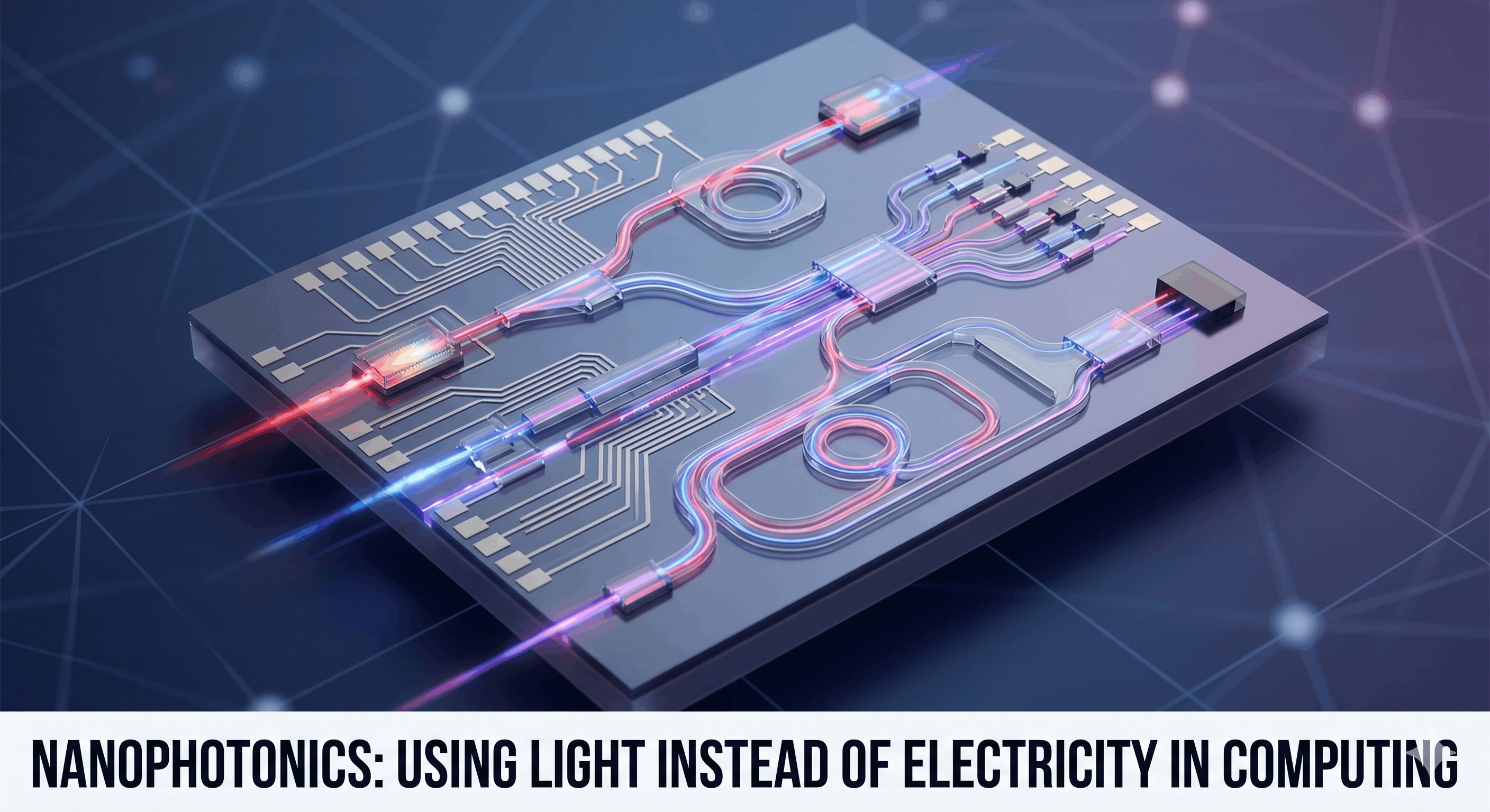
The history of computing has been a relentless race toward miniaturization. For decades, we have followed Moore’s Law, doubling the number of transistors on a silicon chip roughly every two years. However, we have hit a physical wall. As electronic components shrink to the size of atoms, they leak energy, generate immense heat, and face the “bottleneck” of electron travel speeds.
To break through this wall, the next era of computing isn’t looking for smaller electrons—it is looking to replace them entirely. Enter Nanophotonics: the science of manipulating light (photons) at the nanoscale to perform the tasks traditionally handled by electricity.
1. The Bottleneck: Why Electrons are Failing Us
Since the invention of the integrated circuit, electricity has been the medium of choice. But electrons have mass and charge, which means they face resistance as they move through copper wires. This resistance creates heat. In modern data centers, nearly 40% of the energy consumed is used simply to cool down the processors.
Furthermore, as we move into the era of 5G, 6G, and massive Artificial Intelligence (AI) models, the “interconnect” becomes a problem. The wires that move data between the processor and the memory cannot keep up with the speed of the processor itself. This is known as the “von Neumann bottleneck.” Light, however, has no mass, travels at the universal speed limit, and generates almost no heat when passing through a transparent medium. Nanophotonics aims to bring the speed of fiber-optic internet (which uses light for long distances) directly onto the computer chip itself.
2. What is Nanophotonics?
Nanophotonics is the study of light’s behavior on the scale of nanometers—where the structures are smaller than the wavelength of the light itself. Traditionally, light was difficult to “squeeze” into tiny spaces because of the diffraction limit. You generally cannot focus light into a spot smaller than half its wavelength (for visible light, this is about 200–300 nanometers).
Nanophotonics uses “tricks” of physics to bypass this limit:
-
Photonic Crystals: Materials with a periodic structure that can “trap” or “steer” light in specific directions, much like a semiconductor controls electrons.
-
Plasmonics: Utilizing the interaction between light and electrons on the surface of metals (like gold or silver) to compress light into tiny volumes far below the diffraction limit.
-
Silicon Photonics: Integrating optical components into standard silicon manufacturing processes, allowing us to build “light-based” computers using existing factory infrastructure.
3. The Components of a Light-Based Computer
To replace an electronic computer, we need optical versions of every component.
Optical Interconnects
Instead of copper wires, chips use waveguides—tiny channels that act like microscopic fiber-optic cables. These can move data at terabit-per-second speeds across a chip with virtually zero energy loss.
Optical Modulators
A modulator is a “gatekeeper” that converts electronic data into optical pulses (1s and 0s). Current research focuses on using materials like Lithium Niobate or Graphene to create modulators that can switch on and off billions of times per second (GHz to THz range).
Optical Transistors (The Holy Grail)
An electronic transistor is a switch. An optical transistor is a device where one beam of light controls the path of another beam of light. While fully “all-optical” general-purpose computers are still in development, researchers have successfully demonstrated logic gates made entirely of light.
4. Nanophotonics in Artificial Intelligence (AI)
One of the most exciting applications for this technology is in AI and Deep Learning. AI models rely on “Matrix Multiplication”—a heavy mathematical task that is very slow for electronic CPUs and GPUs.
Optical Neural Networks (ONNs) use light to perform these calculations. Because light beams can overlap without interfering (a property called superposition), an optical chip can perform thousands of multiplications simultaneously at the speed of light. Companies and research groups are currently testing “Photonic Tensor Cores” that can train AI models 100 times faster than current hardware while using a fraction of the power.
5. Clinical and Biomedical Applications: The “Lab-on-a-Chip”
While nanophotonics is revolutionizing computing, its impact on medicine and clinical studies is equally profound. By shrinking optical sensors to the nanoscale, we are entering the era of Biophotonics.
Non-Invasive Clinical Monitoring
Current clinical research is exploring nanophotonic sensors that can be placed under the skin or integrated into wearables to monitor glucose levels, oxygen saturation, and even specific cancer biomarkers in real-time. These sensors use Surface Plasmon Resonance (SPR) to detect the presence of a single molecule by observing how it changes the behavior of light on a metallic surface.
Diagnostic Speed
In clinical trials for rapid diagnostics (such as for viral infections like COVID-19 or flu), nanophotonic chips have demonstrated the ability to provide results in minutes rather than hours. These “Lab-on-a-Chip” devices use light to scan a blood or saliva sample, identifying pathogens with the same accuracy as a full-scale laboratory.
Neural Probes
In neuroscience, nanophotonic “needles” are being used in clinical studies to stimulate specific neurons using light (optogenetics) without the heat damage that traditional electrical probes might cause.
6. Advantage–Risk Assessment
Advantages
-
Extreme Speed: Data moves at the speed of light, potentially reaching processing speeds in the Petahertz (PHz) range.
-
Energy Efficiency: Photons do not generate heat through resistance. This could reduce global data center energy consumption by up to 90%.
-
Bandwidth: Light can carry data on different “colors” (wavelengths) simultaneously through the same path, a process called Wavelength Division Multiplexing (WDM).
-
Low Latency: Critical for autonomous vehicles, high-frequency trading, and real-time AI processing.
Risks and Challenges
-
Manufacturing Complexity: Photonic structures must be incredibly precise. A deviation of even 5–10 nanometers can ruin an optical waveguide.
-
The “Size” Problem: While we can make electronic transistors 2–3 nanometers wide, optical components are still significantly larger (hundreds of nanometers) due to the nature of light waves.
-
Interoperability: Most of our world is still electronic. The energy cost of constantly converting light back into electricity (and vice-versa) can sometimes cancel out the benefits of the optical speed.
-
Signal Degradation: Light can scatter or be absorbed if the materials aren’t perfectly pure, leading to signal loss.
7. Current Research Frontiers
The global research community is currently focused on three major “Breakthrough Zones”:
-
Topological Photonics: Researchers are creating “one-way streets” for light. By using specific geometric designs, they can force light to move around corners and imperfections without reflecting back, making chips much more durable.
-
2D Materials: Integrating materials like Graphene and Transition Metal Dichalcogenides (TMDCs) with silicon to create ultra-fast light detectors and emitters that are only one atom thick.
-
Quantum Nanophotonics: Using nanophotonic circuits to move and process “qubits” (quantum bits) in the form of single photons. This is seen as a leading path toward building a scalable, room-temperature quantum computer.
8. Conclusion: A Bright Future
Nanophotonics is more than just a technical upgrade; it is a fundamental shift in how we process information. While we may not have an “all-optical” laptop in our bags in the next five years, the “hybrid” era has already begun. Our data centers, AI training hubs, and medical diagnostic tools are increasingly powered by light.
As we reach the physical limits of what electricity can do, nanophotonics ensures that our thirst for faster, smarter, and greener technology can still be quenched. The future of computing isn’t just bright—it’s made of light.