
Recently added item(s)
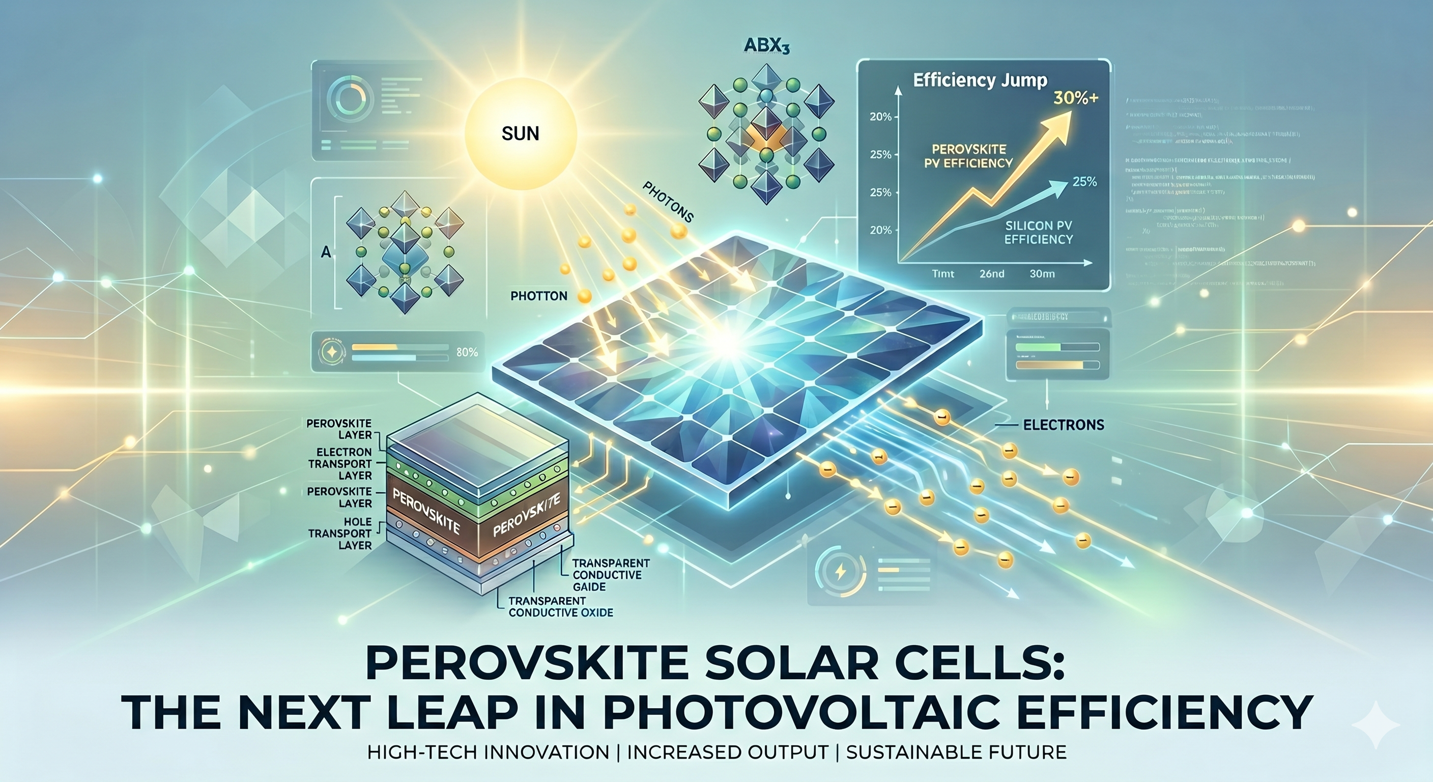
The global transition to renewable energy is accelerating, and at the heart of this movement lies solar power. For decades, traditional silicon-based solar panels have dominated the landscape, silently turning sunlight into electricity on rooftops and in vast solar farms. While silicon has served us well, the scientific community has been chasing a “holy grail”: a new material that is cheaper to produce, more efficient at capturing sunlight, and versatile enough to be used anywhere.
Enter perovskites.
In the world of material science and photovoltaics (PV), “perovskite” is perhaps the most exciting word of the last decade. It doesn’t describe a specific chemical element but rather a unique crystal structure. In a remarkably short period, solar cells utilizing this structure have skyrocketed in efficiency, moving from laboratory curiosities to genuine challengers to silicon’s throne.
This blog post will explore the science behind perovskite solar cells, delve into the current breakthroughs, objectively analyze the risks and rewards, and highlight how this technology is moving from the lab bench to real-world pilot tests—the engineering equivalent of “clinical trials.”
What are Perovskites and Why Do They Absorb Light So Well?
The name “perovskite” (pronounced puh-ROV-skite) was originally given to a specific mineral discovered in Russia in 1839. Today, scientists use it to describe a class of synthetic materials that share the same $ABX_3$ crystal architecture as that original mineral. Imagine a complex molecular cage where atoms are precisely arranged in cubes and octahedrons. This specific arrangement grants the material extraordinary optical and electrical properties.
The Science of Absorption
A good solar cell material must do two things well: absorb photons (light particles) and move the resulting excited electrons effectively to create an electric current. Perovskites are superstars at both.
-
Direct Bandgap: Unlike silicon, most perovskites possess a “direct bandgap.” This means that when a photon hits the material, it can very easily promote an electron to a state where it can conduct electricity, requiring very little material thickness to absorb almost all available sunlight.
-
Long Electron Lifetimes: Once an electron is excited by sunlight, it needs to travel to the battery or grid connection before it settles back down and loses its energy as heat. In perovskites, electrons remain in this excited, “available” state for an exceptionally long time and can travel long distances within the crystal without getting stuck.
The Race for Efficiency: Breaking Records
The defining characteristic of the perovskite revolution is the unprecedented speed of its development.
Silicon solar cells took over 60 years to improve their laboratory efficiency from 4% to the 26-27% range seen today. Perovskite solar cells achieved this same leap in approximately 15 years. In the early 2010s, their efficiency hovered around 3-4%. As of early 2026, certified laboratory efficiencies for single-junction perovskite cells have surpassed 26%, effectively catching up with silicon.
However, the true excitement lies in a technology that merges the old with the new.
The Tandem Solution: 1+1 = 3 (Well, Almost)
Scientists realized that they don’t have to choose between silicon and perovskites. They can stack them. This architecture is known as a Tandem Solar Cell.
Sunlight is composed of different colors (wavelengths), each carrying a different amount of energy. Silicon is excellent at absorbing lower-energy red and infrared light but lets higher-energy blue light pass through or converts it inefficiently.
Perovskites can be chemically “tuned” during manufacturing to absorb specific parts of the light spectrum perfectly. In a typical tandem configuration:
-
Top Layer (Perovskite): A perovskite layer is tuned to absorb high-energy blue and green light. It sits on top because it is semitransparent to other colors.
-
Bottom Layer (Silicon): The lower-energy red and infrared light passes through the perovskite top layer and is captured by a traditional silicon cell underneath.
By combining these two materials, a single solar panel can capture a much broader spectrum of sunlight, shattering the theoretical limits of single-junction cells. In laboratory settings, Perovskite-on-Silicon tandem cells have already achieved certified efficiencies exceeding 33.9%. This is not just an incremental step; it is the “next leap” in photovoltaic history.
The Engineering “Clinical Trials”: Scaling Up to Reality
It is one thing to create a perfect, tiny square centimeter of perovskite in a pristine laboratory. It is entirely another to produce square meters of durable panels that can survive 25 years in the Arizona desert or the rainy Netherlands.
The industry is currently in the crucial phase of transition, moving from “lab to fab” (laboratory to fabrication). These pilot projects and initial manufacturing lines serve as the engineering equivalent of clinical trials, testing real-world performance, manufacturing consistency, and durability.
Case Studies in Commercialization (2024-2026)
-
Oxford PV (UK/Germany): Oxford PV has been a pioneer in tandem technology. They have established a pilot production line in Germany, producing full-sized silicon-perovskite tandem cells. Their panels are undergoing rigorous outdoor testing, proving their ability to withstand environmental stress while delivering significantly higher energy yields than standard silicon. By 2025, they began delivering commercial-grade tandem panels to initial partners for utility-scale testing.
-
Hanwha Qcells (South Korea/USA): This major silicon manufacturer is heavily investing in tandem research. They are building a pilot production line in South Korea to develop perovskite-silicon tandem cells and modules, aiming to commercialize the technology and upgrade their existing global manufacturing infrastructure.
-
Saule Technologies (Poland): Focused on flexible, single-junction perovskites using inkjet printing. They have deployed initial “field trials” on the facades of commercial buildings, testing flexible, semitransparent perovskite “energy blinds” that both shade the building and generate power.
-
Other Players: Companies like Swift Solar and Caelux (USA), Longi and JinkoSolar (China), are all engaged in their own engineering scale-up trials, competing to be the first to deliver stable, high-efficiency tandem modules to the mass market.
The Balanced View: Advantages vs. Risks
While the potential is staggering, we must objectively assess the hurdles that remain.
The Advantages (The Rewards)
-
Ultimate Efficiency: The ability of tandem cells to surpass 30% efficiency drastically reduces the “levelized cost of energy” (LCOE). You get much more power from the same land area or rooftop space.
-
Low-Cost Manufacturing: Unlike silicon, which requires high-purity material and extremely high-temperature processing (over 1000°C), many perovskites can be manufactured using “solution processing”—like printing newspapers. They can be coated, painted, or inkjet-printed onto surfaces at relatively low temperatures (under 200°C), promising significantly lower production costs once scaled.
-
Versatility and Lightweight: Perovskites can be made flexible, lightweight, and even semitransparent. This opens up entirely new markets that silicon cannot reach, such as building-integrated photovoltaics (BIPV)—power-generating windows and facades—and integration into electric vehicles or Internet of Things (IoT) devices.
The Risks and Challenges (The Roadblocks)
-
Long-Term Stability (The Achilles Heel): This is the biggest obstacle. Standard silicon panels are guaranteed for 25-30 years. Early perovskites would degrade in hours or days when exposed to moisture, oxygen, heat, or UV light. While research into stabilization, encapsulation (sealing the panels), and new perovskite chemistries (e.g., using all-inorganic structures or 2D/3D perovskite mixtures) has dramatically improved lifetimes, proving 25-year stability under outdoor conditions remains the critical focus of current “clinical trials.”
-
Toxicity and Environment (Lead Content): The most efficient perovskites currently contain lead. While the amount of lead is tiny (much less than in a standard lead-acid car battery), it still raises environmental concerns regarding end-of-life disposal or potential leakage if a panel breaks. Researchers are actively working on lead-free alternatives (using tin or bismuth), but they currently lag significantly in efficiency. The industry consensus is that efficient lead-based perovskites can be commercialized safely through robust encapsulation and dedicated “take-back and recycling” programs for old panels.
-
Scalability (Lab-to-Fab Consistency): Producing a flawless crystal on a 1 $cm^2$ lab sample is different from coating a 1.5 $m^2$ panel without any defects. Maintaining uniformity and efficiency across large areas using industrial printing or coating methods is a complex engineering challenge that is being solved during current pilot trials.
The Outlook: Are Perovskites the Future?
The short answer is: Most likely, yes.
We are witnessing a paradigm shift. The physics of perovskites is too powerful to ignore. The question is no longer if perovskites will become commercial, but when and in what form.
We will likely see a tiered introduction to the market:
-
Premium Markets (Next 1-3 years): Initially, Perovskite-on-Silicon tandem panels will enter the market as high-efficiency, premium products for residential rooftops or space applications where efficiency is worth a higher price.
-
Specialty Markets: Flexible and semitransparent perovskites will find niches in BIPV and portable power.
-
Mass Market (End of decade): As durability is proven and manufacturing scales up, tandem technology could become the new standard for utility-scale solar farms, ultimately replacing single-junction silicon by delivering significantly cheaper solar energy.
The remaining stability and manufacturing hurdles are significant, but they are engineering problems, not fundamental physics problems. With the global scientific community and major industrial players focused on the solution, the “next leap” in photovoltaic efficiency is well within our grasp, promising to accelerate the clean energy future.