
Recently added item(s)
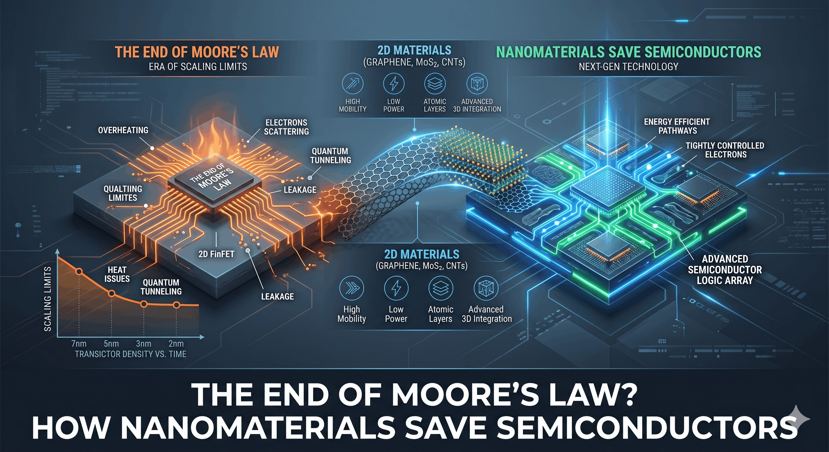
For more than half a century, the technology industry has marched to the beat of a single, relentless drum: Moore’s Law. In 1965, Gordon Moore, the co-founder of Intel, predicted that the number of transistors on a microchip would double approximately every two years, while the cost of computers would be halved. For decades, this prediction held remarkably true, powering the transition from room-sized mainframes to the supercomputers we now carry in our pockets.
However, as we venture deeper into the 2020s, the drumbeat is slowing. We have reached a point where transistors are so small—measured in just a few nanometers—that we are bumping up against the fundamental laws of physics. At this scale, silicon, the bedrock of the digital age, begins to fail. Electrons start “leaking,” heat becomes unmanageable, and the traditional methods of shrinking components simply stop working.
Is this the end of progress? Not quite. A new hero has emerged from the laboratory: Nanomaterials. By moving beyond traditional silicon and embracing materials engineered at the atomic level, we aren’t just saving Moore’s Law; we are reinventing the very foundation of computing.
The Silicon Wall: Why Size Matters
To understand why we need nanomaterials, we first have to understand why silicon is struggling. A transistor acts as a tiny switch. When it’s “on,” current flows; when it’s “off,” it stops. As we shrink these switches to the size of a few dozen atoms, two major problems arise:
-
Quantum Tunneling: At the 3nm or 2nm scale, the barriers in a silicon transistor become so thin that electrons can simply “disappear” from one side and reappear on the other. This is a quantum mechanical effect that makes the switch impossible to turn off, leading to massive energy waste and errors.
-
Thermal Management: Packing billions of tiny switches into a small space generates immense heat. In a modern high-end chip, the power density can rival that of a nuclear reactor surface. Silicon is a decent thermal conductor, but at these densities, it simply cannot shed heat fast enough, leading to “dark silicon”—parts of the chip that must remain turned off to prevent the hardware from melting.
The Graphene Revolution and 2D Materials
If silicon is a tired marathon runner, Graphene is the Olympic sprinter. Consisting of a single layer of carbon atoms arranged in a hexagonal lattice, graphene is the thinnest, strongest, and most conductive material known to man.
Beyond Graphene: The Rise of TMDs
While graphene is a superstar for conductivity, it has a fatal flaw for transistors: it lacks a “bandgap.” A bandgap is essentially the energy barrier that allows a material to be turned off. Without it, a graphene transistor is always “on.”
This has led researchers to a broader class of 2D materials known as Transition Metal Dichalcogenides (TMDs), such as Molybdenum Disulfide (MoS2). These materials are only a few atoms thick, like graphene, but they possess a natural bandgap.
-
Current Research Insight: In 2024 and 2025, pilot studies by leading semiconductor consortiums have successfully integrated MoS2 layers onto standard silicon wafers. This “hybrid” approach allows the chip to benefit from the ultra-thin nature of TMDs—reducing quantum tunneling—while maintaining compatibility with existing manufacturing plants.
Carbon Nanotubes (CNTs): The 3D Solution
If 2D materials are the future of the surface, Carbon Nanotubes (CNTs) are the future of structure. Think of a CNT as a sheet of graphene rolled into a seamless cylinder.
CNTs are exceptional because they can carry significantly more current than copper or silicon while generating less heat. More importantly, they allow for 3D Integration. Traditional chips are flat (2D), but CNT-based transistors can be stacked in multiple layers without the heat issues that plague silicon.
-
The “N3XT” Architecture: Recent industrial research into the N3XT (New Computing Subsystem with Transistor-and-Memory) architecture uses CNTs to interleave layers of logic and memory. This eliminates the “memory wall”—the slow process of moving data between the processor and the RAM—resulting in a 1,000x improvement in energy-efficiency for AI tasks.
Gate-All-Around (GAA) and the Role of Nanowires
As we move toward the 2-nanometer node and beyond, the physical shape of the transistor is changing. For years, we used “FinFETs” (transistors that look like fins). Now, we are moving to Gate-All-Around (GAA) transistors using Nanowires or Nanosheets.
In a GAA transistor, the “gate” (the part that controls the switch) wraps completely around the channel (the part the current flows through). By using nanomaterials to create these wires, we achieve much tighter control over the electron flow. This design virtually eliminates the “leakage” that caused the silicon wall in the first place.
Advantage vs. Risk: The Great Semiconductor Gamble
Moving to a post-silicon world is not a simple “plug-and-play” process. It involves a complex assessment of rewards versus existential risks for the tech industry.
The Advantages
-
Energy Efficiency: Nanomaterial-based chips could extend smartphone battery life from one day to one week.
-
Performance: We can continue to scale AI and machine learning models that require trillions of operations per second without requiring their own dedicated power plants.
-
Miniaturization: Enabling the next generation of “Edge AI”—powerful intelligence inside tiny sensors, medical implants, and wearable devices.
The Risks and Challenges
-
Fabrication Costs: Building a new semiconductor fab (factory) for nanomaterials can cost upwards of $20 billion. The economic risk of a failed material transition is enough to bankrupt even giant corporations.
-
Material Purity: Carbon nanotubes are notoriously difficult to “sort.” You often get a mix of metallic and semiconducting tubes, and even a 0.01% impurity can ruin a multi-billion dollar chip.
-
Environmental Impact: While nanomaterials can make devices more efficient, the process of synthesizing carbon nanotubes and TMDs often involves rare-earth catalysts and high-energy processes that need to be carefully managed to be “green.”
Current “Field Studies” and Reliability Testing
While semiconductors don’t undergo “clinical trials” in the medical sense, they undergo Reliability and Accelerated Life Testing (ALT). Recent data from 2025 research cycles has highlighted a phenomenon called “Contact Resistance.”
When you connect a macroscopic metal wire to a microscopic nanomaterial, the resistance at that junction can be very high. This has been the “silent killer” of many nano-prototypes. However, a breakthrough study in early 2026 demonstrated that using Metal Powders (specifically Nickel and Tungsten alloys) to create “top-contacts” can reduce this resistance by 40%, finally making these materials commercially viable for high-performance servers.
Sustainability and the Future of the Industry
Moore’s Law was always about more than just speed; it was about efficiency. As we look toward 2030, the semiconductor industry is under pressure to reach Net Zero.
Nanomaterials offer a path to “Circular Electronics.” Because carbon-based materials can be synthesized from organic sources and are theoretically more durable, we could see a shift away from the “disposable tech” culture. A chip that doesn’t overheat is a chip that lasts longer, reducing the millions of tons of e-waste generated every year.
Conclusion: A New Era of Discovery
Moore’s Law is not ending; it is evolving. We are graduating from the era of “brute-force” shrinking into an era of Atomic Engineering.
By harnessing the strange and wonderful properties of graphene, nanotubes, and nanosheets, we are doing more than just saving our gadgets. We are creating the hardware capable of solving the world’s most complex problems—from climate modeling to personalized medicine. The transition will be difficult and expensive, but as the limits of silicon become clear, the tiny world of nanomaterials is our only way forward.
The digital future is no longer just written in silicon. It is being printed, grown, and layered, one atom at a time.