
Recently added item(s)
The world of technology is governed by a simple rule: smaller is often better. For decades, Micro-Electro-Mechanical Systems (MEMS) have been the unsung heroes of the digital age. They are the tiny accelerometers that rotate your smartphone screen, the pressure sensors in your car’s tires, and the microscopic mirrors in digital projectors. However, as we push toward the limits of physics, traditional silicon-based MEMS are facing a “size wall.”
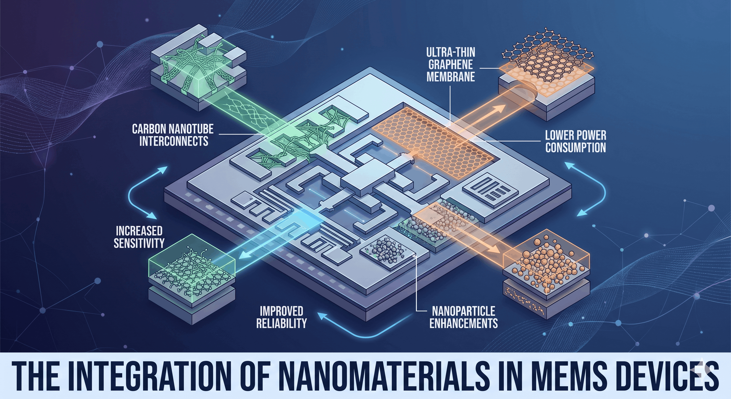
To break through, engineers are integrating nanomaterials—substances engineered at the scale of atoms—into these devices. This marriage of MEMS and nanotechnology is creating a new class of “Nano-Electro-Mechanical Systems” (NEMS) that are more sensitive, more durable, and vastly more efficient than anything we have seen before.
1. Understanding the Foundation: What are MEMS?
Before diving into the “nano” aspect, we must understand the “micro.” MEMS are integrated devices that combine mechanical elements, sensors, actuators, and electronics on a common silicon substrate. They bridge the gap between the physical and digital worlds by converting mechanical movement (like a vibration or a tilt) into an electrical signal.
Traditionally, MEMS are made using silicon. Silicon is excellent for electronics, but at the micro-scale, it has mechanical limitations. It can be brittle, and as devices get smaller, the “surface-to-volume ratio” increases. This means that forces like friction and static electricity (stiction) start to dominate, often causing the tiny moving parts to get stuck or wear out.
2. The Nanomaterial Upgrade: Why Go Small?
Nanomaterials—such as graphene, carbon nanotubes (CNTs), nanowires, and MXenes—possess extraordinary properties that bulk silicon lacks. When we integrate these into MEMS, we aren’t just making the devices smaller; we are fundamentally changing how they behave.
Graphene: The Ultimate Membrane
Graphene is a single layer of carbon atoms arranged in a 2D lattice. In MEMS, it acts as a near-perfect membrane. It is incredibly strong yet flexible, and because it is only one atom thick, it is extremely sensitive to changes in pressure or mass. A graphene-based MEMS sensor can detect the weight of a single molecule landing on its surface.
Carbon Nanotubes (CNTs)
CNTs are essentially rolled-up sheets of graphene. They offer the highest strength-to-weight ratio of any known material. In MEMS actuators, CNTs can provide the structural integrity needed to withstand millions of cycles of movement without fatigue.
Metallic Nanoparticles and Nanowires
Integrating gold, silver, or nickel nanoparticles into the conductive paths of a MEMS device allows for better electrical conductivity and reduced heat generation. This is crucial for devices that must operate at high frequencies, such as those used in 5G and satellite communications.
3. Key Integration Techniques
Integrating a material that is only a few nanometers wide into a micro-scale device is an immense engineering challenge. Several methods have emerged as the industry standard:
-
Chemical Vapor Deposition (CVD): Growing nanomaterials like graphene or CNTs directly onto the silicon wafer during the manufacturing process.
-
Self-Assembly: Using chemical properties to encourage nanomaterials to “organize themselves” into specific patterns on a device.
-
Nanoprinting: Using specialized “functional inks” containing nanomaterials to print sensors directly onto a MEMS structure. This is particularly useful for flexible electronics.
4. Current Research and Technological Trends
Research in the integration of nanomaterials is currently focused on solving the “reliability gap.” While a laboratory prototype might work perfectly, mass-producing millions of nano-integrated MEMS devices requires extreme precision.
High-Frequency Resonators
Recent studies are looking into using carbon nanotubes as “nanomechanical resonators.” These are essentially tiny tuning forks that vibrate at gigahertz frequencies. They are expected to replace the bulky quartz crystals currently used in wireless communication, allowing for even smaller and faster 6G devices.
Artificial Intelligence (AI) Integration
A major trend is the development of “Edge AI” sensors. By integrating nanomaterials that can process signals locally (neuromorphic computing), a MEMS sensor wouldn’t just detect a vibration; it would “understand” what that vibration means—such as identifying a specific mechanical failure in a factory—without sending data to the cloud.
5. Clinical and Biomedical Applications: The “Lab-on-a-Chip”
Perhaps the most exciting “clinical” application of nano-MEMS is in the medical field. These devices are the backbone of the “Lab-on-a-Chip” (LoC) revolution.
Non-Invasive Diagnostics
Clinical research is currently testing MEMS sensors integrated with graphene to detect biomarkers in human sweat or breath. For example, a MEMS-based “electronic nose” can detect volatile organic compounds associated with lung cancer or diabetes at concentrations as low as parts-per-billion.
Targeted Drug Delivery
Researchers are developing MEMS-based implants that use nano-membranes to release precise doses of medication over months or years. Unlike traditional pills, these devices can be “triggered” by an external signal to release a dose only when needed, reducing side effects and improving patient compliance.
Neural Interfaces
In neuroscience, nano-MEMS probes are being used in clinical studies to record the electrical activity of individual neurons. The use of nanomaterials makes these probes more “biocompatible,” meaning the body’s immune system is less likely to reject them, which is a major hurdle for long-term brain-computer interfaces.
6. Advantage–Risk Assessment
As with any disruptive technology, there is a balance between its potential and its risks.
Advantages
-
Sensitivity: Nano-MEMS can detect forces and masses that are invisible to traditional sensors.
-
Power Efficiency: These devices require significantly less energy to operate, which is vital for the Internet of Things (IoT) where devices must run on batteries for years.
-
Size: Reduction in volume allows for integration into wearables, smart clothing, and even the human body.
-
Multi-functionality: A single nano-integrated chip can often measure pressure, temperature, and chemical composition simultaneously.
Risks and Challenges
-
Stiction and Friction: At the nanoscale, surfaces like to stick together. If a tiny mechanical arm in a MEMS device touches a surface, it may never come off due to Van der Waals forces.
-
Toxicity and Environment: We are still learning about the long-term environmental and health impacts of nanomaterials. If a medical MEMS device breaks down inside the body, how do the nanoparticles affect our cells?
-
Cost of Manufacturing: While the materials themselves are becoming cheaper, the specialized cleanrooms and equipment needed to integrate them are incredibly expensive.
-
Reliability: Nanomaterials can be sensitive to environmental changes like humidity or oxidation, which can cause the sensor’s accuracy to “drift” over time.
7. The Road Ahead: From MEMS to NEMS
We are currently in a transition phase. The industry is moving from traditional MEMS to NEMS (Nano-Electro-Mechanical Systems). In the next decade, we expect to see “zero-power” sensors that harvest energy from the environment (vibrations or heat) to power themselves indefinitely.
The integration of nanomaterials isn’t just an “add-on” for MEMS; it is the fundamental engine that will drive the next generation of smart cities, autonomous vehicles, and personalized medicine.